- Joined
- Dec 11, 2018
- Messages
- 1,222
- Trophies
- 0
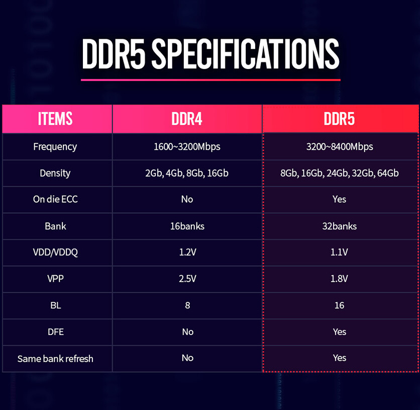
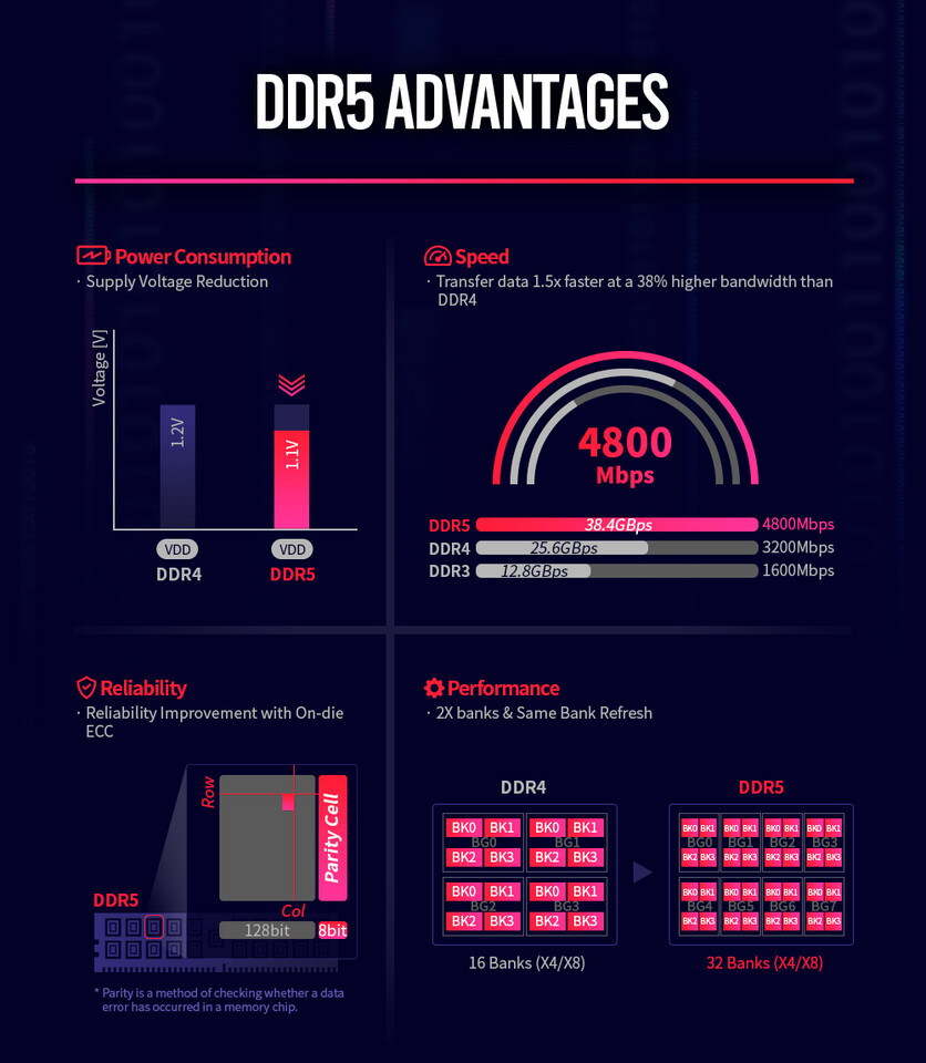
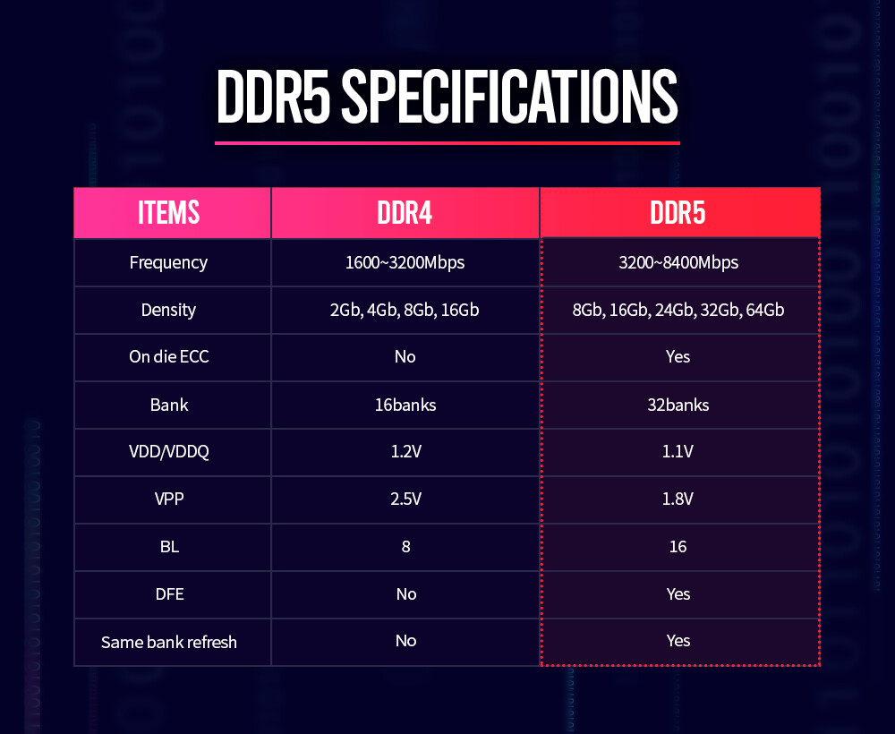
SK Hynix has today posted an update on their blog about the upcoming DDR5 memory, which they have developed in co-respondence with JEDEC's progression of the standard. They have noted a few key things, among which some of the most interesting are features like the maximum speed of 8400 MHz. The DDR5 standard is very flexible, allowing manufacturers to release their chips with frequencies ranging anywhere from 3200-8400 MHz. While the lowest speed is 3200 MHz, manufacturers are starting with 4800 MHz chips and building their way up from there. The minimum density of a single DDR5 die is 8 Gb, while the maximum is 64 Gb, quadrupling the maximum capacity of DDR4 dies.
Perhaps one of the biggest changes besides capacity and speed improvements is the addition of Error-Correcting Code (ECC) support for memory. This feature is now not exclusive to special dies, like with DDR4, but rather is built inside every die. The DDR5 memory chips use 32 banks, split into 8 bank groups, which is designed to provide as much bandwidth as possible. Burst Lenght is doubled to 16, compared to 8 of DDR4, so memory access availability is better. Operating Voltage is decreased to 1.1 V, from the previous 1.2 V of DDR4, resulting in an overall decrease of 20% of power consumption. The mass production of SK-Hynix's DDR5 chips will start this year, however, timing is unknown.
SK Hynix Unveils DDR5 Memory Details, Production to Start This Year
SK Hynix has today posted an update on their blog about the upcoming DDR5 memory, which they have developed in co-respondence with JEDEC's progression of the standard. They have noted a few key things, among which some of the most interesting are features like the maximum speed of 8400 Mbps. The...